集成TVS具有浪涌保护功能的过压保护OVP负载开关——AW328XX 系列
特性
浪涌保护
IEC 61000-4-5: >100V
集成Rdson 仅28m(typ.)的nFET 开关
4.5A 连续电流能力
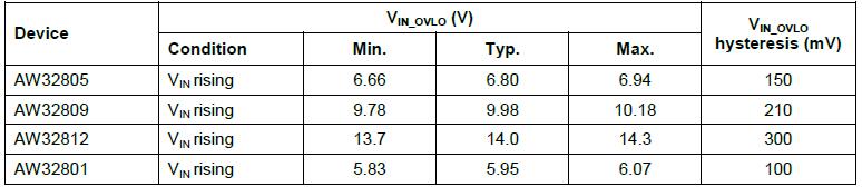
过压保护(OVP)默认阈值
AW32801: 5.95V
AW32805: 6.8V
AW32809: 9.98V
AW32812: 14V
过压保护阈值可调范围4~20V
IN 端系统级ESD 保护
IEC 61000-4-2 接触放电:±8kV
IEC 61000-4-2 空气放电:±15kV
输入最大直流耐压29V
过压关断响应时间仅125ns(typ.)
过温保护(OTP)
欠压关断(UVLO)
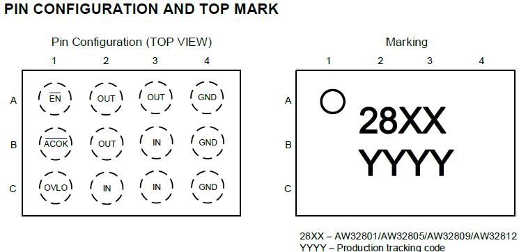
纤小的1.34mm x 1.78mm WLCSP-12 封装
概要
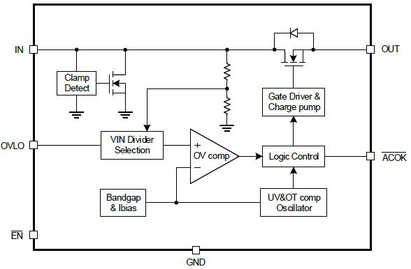
AW328xx 系列是集成有TVS防浪涌功能的OVP 芯片,芯片内部在IN 端并联了钳位电路,能够抑制高达100V 的浪涌电压。
AW328xx 内部集成了Rdson 仅28mohm.(typ.)的nFET 负载开关。当IN 端电压超过OV 阈值,直通功率管迅速关断,防止OUT 端所连接的器件被过压损坏。IN 端直流耐压达到29V。
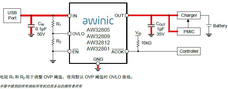
AW328xx 系列过压保护阈值默认为5.95V( AW32801 )、6.8V ( AW32805 )、9.98V(AW32809)、14V(AW32812),也可通过在OVLO 引脚外接分压电阻调节,可调范围4~20V。
AW328xx 具有漏端开路输出信号ACOK,当VIN_UVLO < VIN < VIN_OVLO且NMOS功率管开启后,ACOK会被拉低,指示芯片正常工作,否则ACOK输出为高阻态。
AW328xx 内置过温保护,防止芯片过热烧毁。
AW328xx 采用纤小的1.34mm x 1.78mmWLCSP-12 封装,符合RoHS 规范,占板面积小。
典型应用图
型号列表
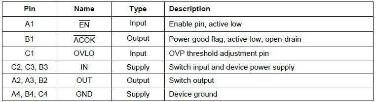
Pin脚分布
功能结构框图
Device Operation
If the AW328xx is enabled and the input voltage is between UVLO and OVP threshold, the internal charge pump begins to work after debounce time, the gate of the nFET switch will be slowly charged high till the switch is fully on. ACOK will be driven low about 30ms after VIN valid, indicating the switch is on with a good power input. If the input voltage exceeds the OVP trip level, the switch will be turned off in about 125ns. If is pulled high, or input voltage falls below UVLO threshold, or over-temperature happens, the switch will also be turned off.
Surge Protection
The AW328xx integrates a clamp circuit to suppress input surge voltage. For surge voltages between VIN_OVLO and VIN_CLAMP, the switch will be turned off but the clamp circuit will not work. For surge voltages greater than VIN_CLAMP, the internal clamp circuit will detect surge voltage level and discharge the surge energy to ground. The device can suppress surge voltages up to 100V.
Over-Voltage Protection
If the input voltage exceeds the OVP rising trip level, the switch will be turned off in about 125ns. The switch will remain off until VIN falls below the OVP falling trip level.
OVP Threshold Adjustment
If OVLO pin is not grounded, and by connecting external resistor divider to OVLO pin as shown in the typical application circuit, between IN and GND, the OVP threshold can be adjusted as following:
The adjustment range is 4V to 20V. When the OVLO pin voltage VOVLO exceeds VOVLO_SEL(0.42V typical), VOVLO is compared with the reference voltage VOVLO_TH (1.2V typical) to judge whether input supply is over-voltage. For example, if we select R1 = 51k兦 and R2 = 12.4k兦, then the new OVP threshold calculated from the above formula is 6.14V.
Output
The device features an open-drain output ACOK, it should be connected to the system I/O rail through a pull-up resistor. If the device is enabled and VIN_UVLO < VIN < VIN_OVLO, ACOK will be driven low indicating the switch is on with a good power input. If OVP, UVLO, or OT occurs, or is pulled high, the switch will be turned off and ACOK will be pulled high.
USB On-The-Go (OTG) Operation
If VIN = 0V and OUT is supplied by OTG voltage, the body diode of the load switch conducts current from OUT to IN and the voltage drop from OUT to IN is approximately 0.7V. When VIN > VIN_UVLO, internal charge pump begins to open the load switch after debounce time. After switch is fully on, current is supplied through switch channel and the voltage drop from OUT to IN is minimum.


